PCB Layout
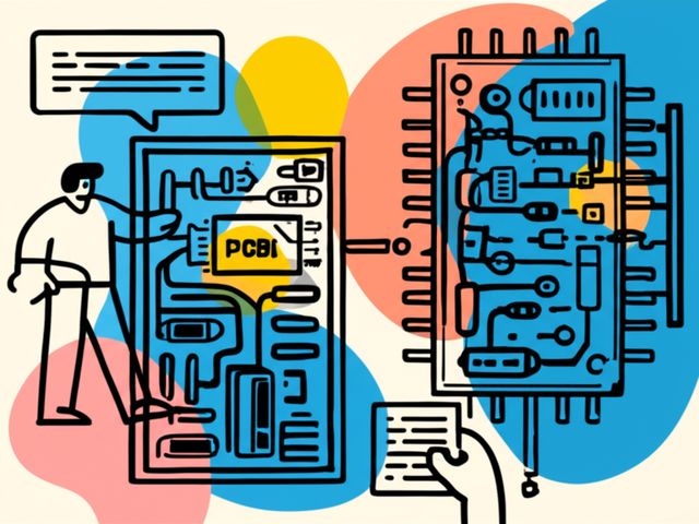
PCB Layout, or Printed Circuit Board Layout, is the process of designing and arranging the components of a printed circuit board (PCB). PCBs are used in a wide variety of electronic devices, from simple gadgets to complex computers. The layout of a PCB is critical to its function, as it determines how the components are connected to each other and how the board will fit into its intended application.
PCB Design Process
The PCB design process typically begins with a schematic diagram, which is a graphical representation of the electrical connections between the components of the board. The schematic diagram is then used to create a layout, which is a physical representation of the board, including the placement of the components, the routing of the traces, and the layout of the board itself.
There are two main types of PCB layouts: single-sided and double-sided. Single-sided layouts have all of the components and traces on one side of the board, while double-sided layouts have components and traces on both sides of the board. Double-sided layouts are more complex to design and manufacture, but they can be more compact and efficient than single-sided layouts.
PCB Manufacturing
Once the PCB layout is complete, it is sent to a PCB manufacturer, who will create the physical board. The manufacturing process typically involves several steps, including: